The fabrication of a prototype IC chip is a highly costly and time-consuming process, requiring significant financial investment and an extended timeline ranging, at least, from several months to even a year for completion.
Tapeout: refers to the final stage of the design process, just before sending it to a semiconductor foundry for fabrication. Imagine, it is like pressing the printing button once the chip is fully designed on the computer
The tape-out of a chip prototype is a very costly and long process. Consequently, it becomes crucial for designers to strive for a successful tape-out without the need for re-design iterations, whenever possible.
In today’s highly competitive market, companies are continuously seeking ways to minimize their time-to-market and launch new products while also reducing costs. On the other hand, research institutes and universities often operate under budget constraints, limiting their ability to engage in multiple tape-outs throughout the year, typically being limited to 1 to 3 tape-outs annually.
Therefore, it becomes imperative for both industry and academia to optimize their design flow, maximize the chances of a successful tape-out, and efficiently utilize their available resources.
A Quick Overview
In the next flow diagram, you have an overview of the full design process for analog integrated circuits with an average estimation of the necessary time for each step for a small project. Although the time needed can vary a lot between different projects and companies, this will give you an approximation.
large and complex projects can extend the design time, especially for the design engineer, up to 6 months or even 1 year, depending on the magnitude. For example, I took part into the design a full inductor-based buck converter, and it needed around a year to be designed.
Picture: Analog Design Flow with approximate timings for a small block or project
Short Description of the Design Steps
Some of the Analog IC Design steps including the layout are here described a bit more in detail:
Design of the Circuit Schematic in Cadence Virtuoso
Ensure that all the simulation are correct and the circuit behaves as desired. On the picture below, you can see a small example of how a simple Cadence schematic looks like:
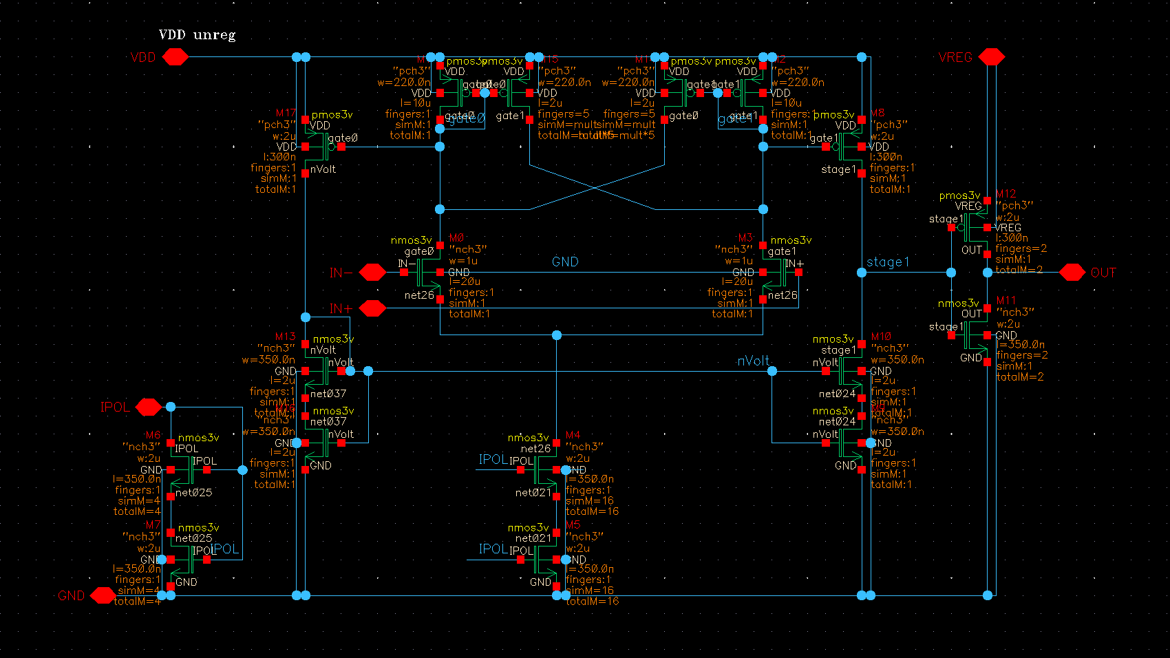
Picture: Example of a Schematic Entry in Cadence Virtuoso EDA Tool
Layout Generation
When fabricating the circuit, each electronic device has a physical structure in real life. For example, a resistor is a long wire of POLY, a MIM capacitor is two metal layer with an insulator in between. Transistors have a more complex structure with doping regions, metals and poly layers. All the devices are set together and routed following the schematic connections. Matched transistors or devices need special care and some additional structures have to be added like guard rings or dummies.
DRC Check
This test is performed usually with the tool Calibre, which is fully integrated in Cadence Layout Environment. Calibre is a software from Mentor Graphics (Now Siemens) and not from Cadence. DRC stands for Design Rules Check.
In this check rules for a proper layout are checked, like space between polygon of the same layers or layers densities. Layers densities (labelled as ‘R’) are ignored here because they are going to be solved later, as it can be seen in the pic below.
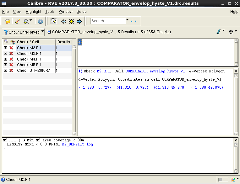
Picture: Snapshot of Siemens Calibre tool after a DRC check
LVS Check
Here the Layout is compared versus the Schematic. The connections between components are exactly as it is drawn in the schematic. Here is where the possible electric shorts are found.
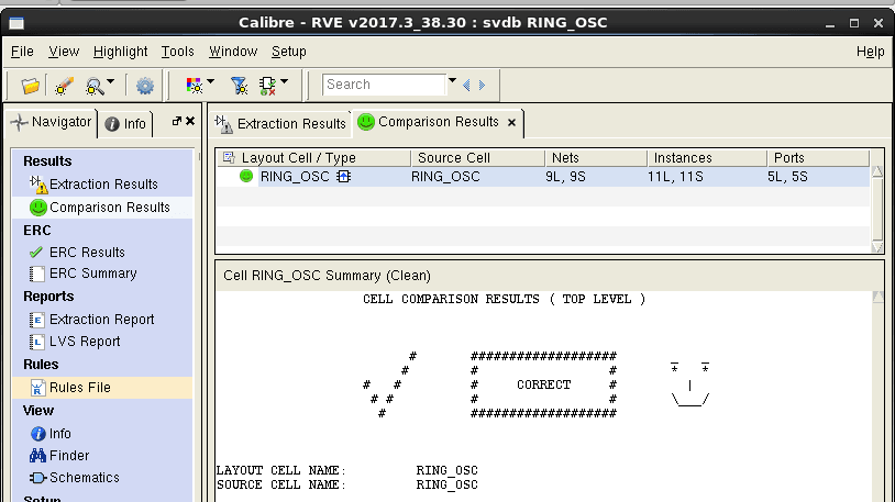
Picture: After LVS using Siemens Calibre EDA tool
Pass the Antenna and Bonding
Wire rules. After both checks (DRC and LVS) are passed, these rules ensure that the chip can be manufactured properly without technical problems. For example, long wires in a single metal layer are not desired or vias from the top layer directly to the gate of a transistor neither.
Floor Planning
The electric pads are connected to the previously designed block. Also if the chip is composed of various blocks, here they are put together. Also, the number of pins and the pin-out is defined.

Picture: Floor Planning of the Block
Dummy Filling
The previously chip layout does not fill the 100% of each metal layer. During the fabrication, it is desired that all the layers are more or less equally filled. This is made, excepting critical regions, automatically with a SKILL script. Here is where the DRC rules errors for “densities” are solved.
Picture: Layout Before Dummies Filling
Picture: Layout After Dummies Filling
DRC and LVS
This check is not strictly necessary, if the previous 3 steps were performed right. But it is a good practice to double-check everything after you may make small changes. An LVS (Layout versus Schematic) with the all the dummies is strongly recommended.
Export to a GDS File
The final version is exported in Cadence and sent to the manufacturer. To do that, go to the CIW window. Then File>> Export >> Stream…

Picture: Export to a GDS File
Send to the Manufacturer (Tape-out)
Once the GDS file is exported, it will be sent to TSMC, which is the real manufacturer.
Wafer Parts
- Chip: The thin and small piece on the wafer where the electrical circuits are embedded. The IC chip.
- Scribe Line: The border between the chip without any electrical circuits. Lines to separate each chip on the wafer.
- TEG (Test Element Group): A chip to test whether it works or not.
- Edge Die: The damaged part. A bigger wafer has less damage than a wafer with a smaller diameter, which also reduces the loss factor.
- Flat Zone: The flat part to distinguish the round wafer structure.
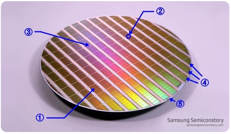
Picture: Wafer Parts (Credit: Samsung Semiconstory)

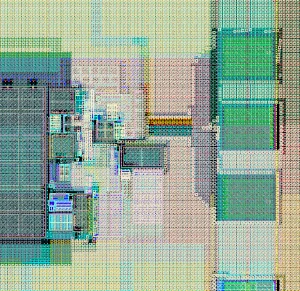
Picture: DSP layout (a) Die photograph of DSP chip in IC Compiler (b) Die photograph of fabricated chip after tape-out (c) The 16-bit fixed-point DSP core.
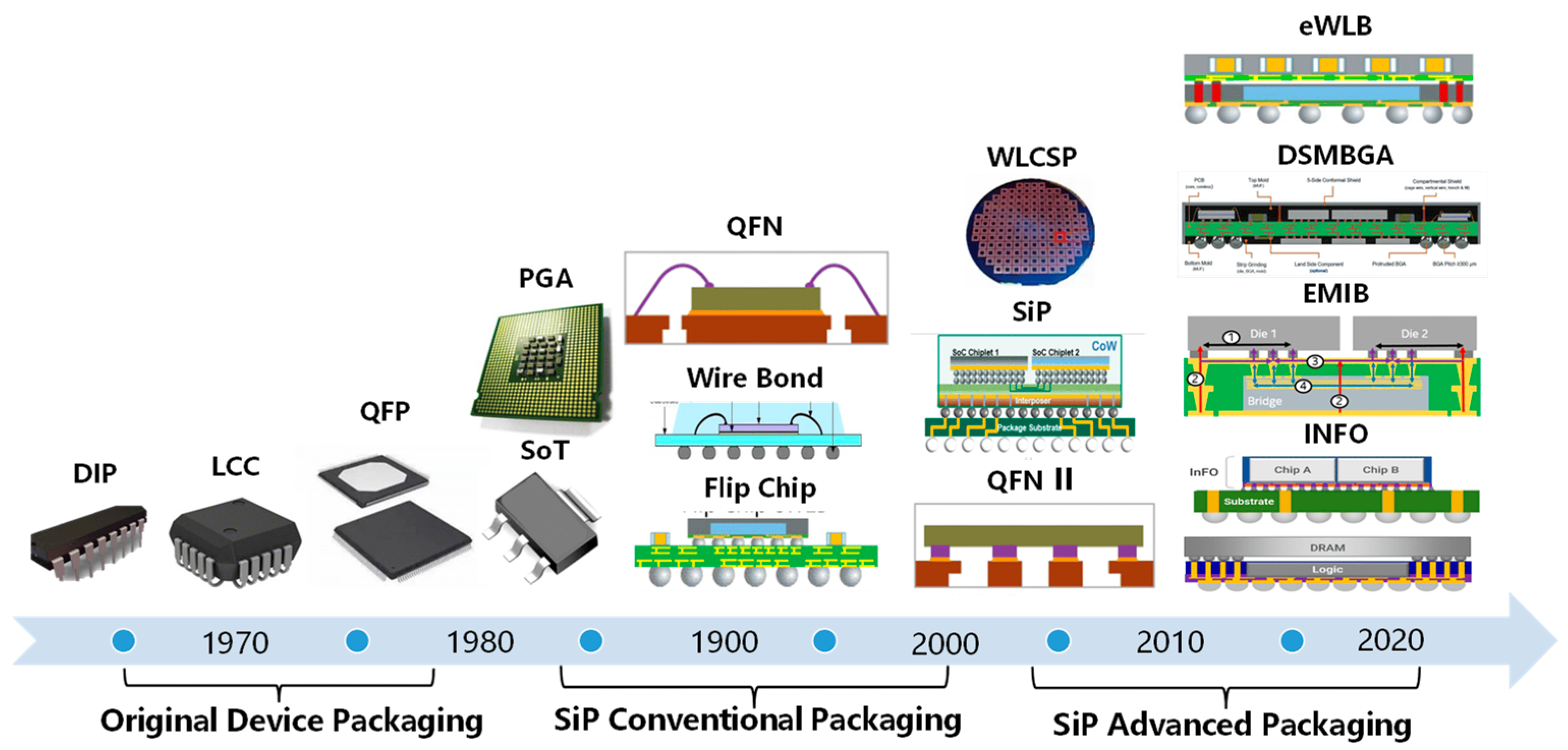
Transistor Density in a Chip and Evolution of IC Packaging – 1970 to 20230
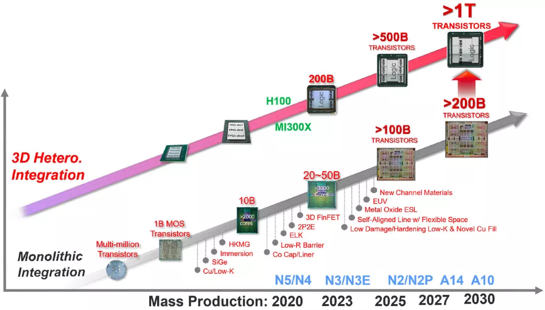
Picture: TSMC working towards a future with trillion-transistor chips, 1nm-class manufacturing
Receive the Chip and Test
After some months you will receive a low number of dies. The elapsed time ranges from 2 to 10 months depending on many factors. Between 20 and 40 units to test. You can decide if you want to encapsulate it into a package or not. Packaging a prototype die, it is not really cheap, and could cost almost the same as the fabrication. For an early stage of prototyping, you may want to only measure the fabricated die on-chip with needles. When you have a more developed prototype, you usually want to include it to a PCB, etc. So in this case, it makes more sense to package.
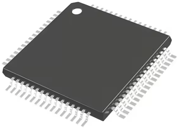
Picture: Finished chip in a Package
Refer https://www.connectronics.com.my/products/types-of-integrated-circuits-ic-electronic-components-5 for more packaging information
Conclusion
In conclusion, this article provided a concise overview of the analog design flow in ICs, with a focus on the often underestimated layout and intermediate steps.
Each of these steps could be explored in much more detail in separate articles, but the intention here was to offer a brief yet informative description with a helpful flow diagram.
This article aims to contribute to spread and broaden the world of analog IC design and inspire further and new designers.